The semiconductor industry stands at the forefront of computational innovation, allowing advancements in information processing, communication, and numerous emerging technologies such as artificial intelligence and electric vehicles. This industry is a global market influenced by geopolitical relationships, supply chain intricacies, and rapidly evolving consumer demand. Starting with the development of the transistor, often deemed the most important invention in the modern age, the semiconductor industry has grown to impact nearly every single electronic device used today. Semiconductor chips can be found in nearly all markets including consumer electronics, healthcare, military, and automotive markets to name a few. The continuous advancement in this industry requires an increasingly important focus on manufacturing robustness and precision, a challenge piezoelectric system have seen success addressing.
Fundamentally, a semiconductor is a material that bridges the gap between insulators that inhibit the flow of electricity due to high resistivity and conductors that encourage the flow of electricity with high conductivity. Compared to traditional charge-carrying metals, semiconducting materials offer precise electrical conductivity control, device miniaturization, and energy efficiency. Germanium, aluminum nitride, and gallium arsenide have been proposed as the leading semiconductor materials; however, silicon has been the preferred material due to availability, cost, and superior performance characteristics.
The manufacturing process of semiconductor chips is complex and includes many interconnected steps, sometimes repeated, that form the desired semiconductor device. This process can split into three stages: Silicon wafer fabrication, front-end die fabrication, and back-end device packaging. Each stage has unique challenges and production steps that require innovative solutions. One challenge is evident across all manufacturing steps: The impact due to the demand for smaller, denser, and faster chips.
Precise Components & Equipment are needed for Precise Wafer Design & Manufacturing
This demand has caused an industry-wide focus on miniaturization that encourages cost reduction and process improvements that define the semiconductor industry. Moore’s Law, named after Gordon Moore who was an Intel engineer and businessman, states that the transistor count on an integrated circuit doubles every two years. This law has held up until recently, as transistor sizes have approached the size of a few atoms wide, challenging the laws of molecular physics. The main concern is quantum tunneling, which disrupts the insulating/conducting properties of neighboring atoms within the transistors. This phenomenon only occurs at sub-nanometer scales and has not been a previous concern.
At a glance, the push for smaller and faster chips appears predictable since technological advancements typically equate to performance increases with smaller form factors. The market demand for faster, smaller, and more economical electronic devices supplements this observation. However, the mechanics behind chip miniaturization are much more nuanced. It may be intuitive to assume that increasing transistor quantity and size increases computational power when spaced traditionally. Although equally spaced transistors lead to increased power, the physical interconnections are longer which increases heat generation while decreasing power efficiency. Therefore, an alternate solution is needed to build complex modern devices and is solved by increasing transistor density. Not only does increasing transistor density save space by minimizing path length but it also reduces operational voltages, thus improving power efficiency. This way a single transistor-dense chip produces more computation operations at cooler temperatures and less power than a less transistor-dense chip twice its size.
Current semiconductor equipment and future innovations require precise and reliable equipment to address the continuing push for miniaturized chips and increasing chip demand. This whitepaper dives into the pivotal role piezoelectric systems play in solving these challenges so that the semiconductor industry can continue to be at the forefront of innovation and advancements in new technologies.
Piezo Solutions for Semiconductor Manufacturing Applications

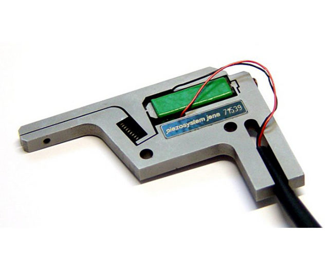
Piezo technology from piezosystem jena is instrumental in the architecture, masking and mask development, testing, inspection, wafer dicing and wafer cutting processes within the semiconductor manufacturing industry. High resolution actuators offer nanometer step-sizes with high repeatability, providing versatility and reliability in wafer and tool positioning. Equally important to performance is reliability, as customers have high throughput demands and cannot afford any downtime. The semiconductor manufacturing components from piezosystem jena are produced and tested to the highest standards within the industry.
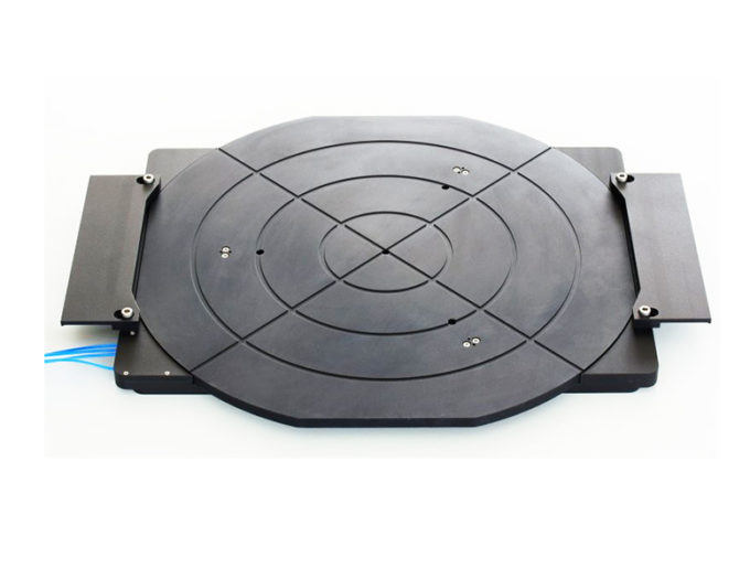
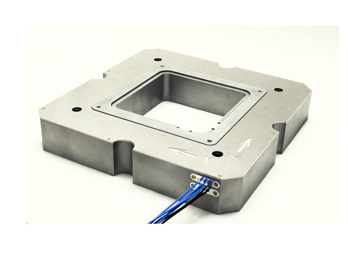
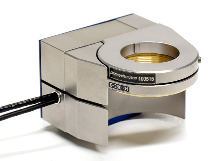
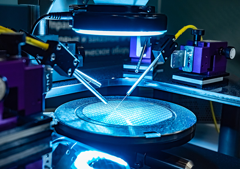
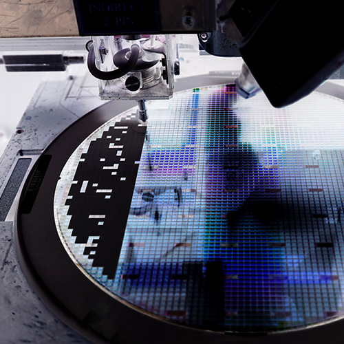
Precise Wafer Design & Inspection Piezo products often designed into semiconductor industry equipment as OEM components include:
- MIPOS Optical Objective Positioners for precise focus and positioning of objectives and inspection tools
- Multi-axis Stages to hold and align wafers and tools for inspection and production
- Fiber Grippers and Fiber Switches for data transfer, testing and switching
- Stack and Ring Actuators for versatile and precise actuation across the manufacturing and testing process
- Fast Steering Mirrors for advanced lithography and wafer dicing
To request a copy of our NEW 22-page whitepaper: Piezoelectric Actuators in the Semiconductor Manufacturing Industry, please click here.